Key words: sarcophagus crystal; series resonance frequency; zero phase method of π network; DDSAD9912
Introduction Quartz crystal resonators (hereafter referred to as quartz crystals) are widely used as time-frequency references and provide synchronization pulses for sequential logic circuits. The quartz crystal test methods mainly include impedance meter method, π-network maximum transmission method, and π-network zero phase method. The π-network zero-phase method is a standard method recommended by the International Electrotechnical Commission (IEC). Π-network zero-phase quartz crystal test equipment has been widely used in developed countries. The typical instrument is a 250B zero-phase test system produced by S&A Company in the United States. Its test frequency range is 0.5 to 200 MHz, and the series resonant frequency test accuracy is ±2 ppm. Impedance quartz crystal test equipment still dominates in China. Impedance type quartz crystal test equipment has the characteristics of low manufacturing cost and simple operation. However, its series resonant frequency measurement range is small and measurement accuracy is low. Therefore, the development of a wide-range, high-precision quartz crystal frequency test system has the practical significance of service production.
The frequency range and accuracy that can be measured by the π-network zero phase method quartz crystal test system directly depend on the frequency sweep signal source of the π network. In order to make the measurement range of the quartz crystal test system reach 20 kHz to 400 MHz, it is necessary to study and design a signal source. The output frequency range of the signal source is 0 to 400 MHz, and the output frequency has high accuracy, high stability, high frequency resolution, and fast frequency switching.
1. π-network zero-phase high-frequency quartz crystal test system design 1.1 Quartz crystal electrical parameter equivalent model Quartz crystal has a piezoelectric effect. When the frequency of the applied alternating electric field is equal to its natural frequency, the quartz crystal will produce a mechanical resonance. This mechanical vibration generates an electrical resonance through the coupling of the piezoelectric effect and the oscillating circuit. In this case, the quartz crystal can be equivalent to the RLC resonant circuit shown in FIG. Among them, C0 is the static capacitance, L1 is the dynamic inductance, Rr is the series resonance resistance, C1 is the dynamic capacitance.

1.2π network zero-phase method quartz crystal frequency test principle IEC recommended π network model shown in Figure 2, π network consists of symmetrical double π-loop, R1, R2 and R3 constitute the input attenuator, R4, R5 and R6 The output attenuators are constructed. Their function is to match the impedance of the pi network with the impedance of the measuring instrument and to attenuate the reflected signal from the measuring instrument. Y is the quartz crystal to be measured. VA is the π network input signal, VB is the π network output signal, the actual measurement pair, constantly changing the input signal frequency, measuring the phase difference between the input signal and the output signal, when the quartz crystal is in the resonant state, the entire π network is pure resistance Sex, the phase difference between the input signal and the output signal is zero. Therefore, the π-network zero-phase method can determine whether the quartz crystal to be measured is in resonance by detecting whether the phase difference between the signals at both ends of the π-network is zero, so as to measure the series resonant frequency of the quartz crystal. When the phase difference between the signals at both ends of the π network is zero, the quartz crystal is in a resonant state, and the quartz crystal series resonant frequency is equal to the π network input signal frequency.
1.3 Test System Design This system is based on the zero-phase method of the Iridium network. It consists of a DDS circuit, a π network circuit, a phase detector circuit, an analog signal processing circuit, a serial port circuit, an LCD circuit, a touch screen circuit, a keyboard circuit, and a 512MB NANDFLASH memory circuit. Etc. Figure 3 is a block diagram of the crystal frequency test system.
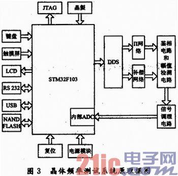
The high-frequency quartz crystal test system uses an ARM chip STM32F103 as a core unit. The STM32F103 core is a 32b Cortex-M3CFU with a maximum operating frequency of 72MHz. STM32F103 is connected with AD9912 of DDS chip through built-in high-speed SPI bus, control AD9912 output frequency sweep signal.
When the crystal to be measured is put into the π network circuit, the phase difference between the input and output signals at the two ends of the π network is different under different sweep signals. The input signal and output signal at both ends of the π network are sent to the phase discrimination circuit respectively, and a voltage signal proportional to the phase difference between the input and output signals at both ends of the π network is obtained at the output of the phase discrimination circuit. The relationship between the output voltage signal of the phase detector circuit and the phase difference of the input signal is shown in FIG. 4 .
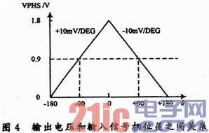
The output voltage signal of the phase detector circuit is converted into a signal suitable for ADC acquisition through a signal conditioning circuit. The signal is captured inside the processor through the 12-bit ADC channel built into the STM32F103. During the measurement process, the frequency of the DDS output signal increases from small to large. The absolute value of the phase difference between the input signal and the output signal at both ends of the π network changes from large to small and gradually approaches zero, and then increases from small to large. However, the ADC's acquisition results increase from small to large and then change from large to small. Therefore, the frequency of the DDS output signal corresponding to this maximum 1.8V is the series resonant frequency of the quartz crystal.
2, DDS technology in the test system 2.1 DDS technology DDS has two prominent features, on the one hand, DDS works in the digital domain, once the frequency control word is updated, the output frequency will be changed accordingly, its frequency hopping rate is high; On the other hand, due to the wide range of frequency control words, the frequency resolution is high. Compared with traditional frequency synthesizers, DDS has the advantages of low cost, low power consumption, high resolution and fast frequency conversion, and is widely used in the field of electronic instrumentation.
The AD9912 is a new DDS chip introduced by Analog Devices in 2007. Its internal clock speed can be as high as 1GSPS, and its 14-bit digital-to-analog converter is integrated, so it can directly output 400MHz signals. The AD9912 uses a 48-bit frequency control word and the output frequency resolution is less than 4μHz. The AD9912 is compatible with a wide variety of system clock inputs. Quartz crystals, crystal oscillators, and external clocks can all be used as their system clock inputs. With an on-chip system clocked phase-locked loop (PLL), the system clock input is allowed down to 25MHz.
2.2 Signal Source Hardware Design I chose ADI's AD9912 as the core of the signal source. STM32F103 controls the AD9912 to output 0 to 400MHz sweep signal through built-in high-speed SPI bus. The working principle of AD9912 is shown as in Fig. 5.

The peripheral circuit of AD9912 is mainly made up of 5 big modules: Power source, clock source, SPI communication interface, start configuration logic, output signal processing circuit.
The power supply of the AD9912 is divided into four major categories: analog 3.3V, digital 3.3V, analog 1.8V, and digital 1.8V. Analog 3.3V and digital 3.3V are isolated from each other through the filter. Analog 1.8V and digital 1.8V are isolated from each other through the filter. The AD9912 reference clock uses a high-performance 25MHz constant-temperature quartz crystal. The AD9912's internal PLL circuit multiplies this reference clock by a factor of 40 to obtain a 1000MHz clock signal as the AD9912's system clock. The 32-pin CLKMODESEL is the clock mode select pin. If a quartz crystal is used as the system clock input, this pin should be grounded. If an oscillator or external clock source is used as the system clock input, the pin should be pulled up to 1.8V. . Since the quartz crystal is selected, the pin is grounded.
The SPI communication interface hardware connection is shown in Figure 6.

The boot configuration logic contains four pins S1, S2, S3, and S4. When S4 is logic 0, the clock mode is selected: the quartz crystal is used as the system clock input, and the AD9912 internal PLL circuit multiplies the clock signal; when S4 is logic 1, the clock mode is selected: the clock signal is input directly from the outside. Therefore, set S4 to logic 0. Eight different logic combinations of S1, S2, and S3 are used to select eight preset 16-bit frequency control words. Allows 8 different frequency signals to be generated without configuring the I/O registers. Since the test system needs a scan signal and does not need a fixed-frequency signal, S1, S2, and S3 are set to logic 0 so that the DDS does not output a signal at startup.
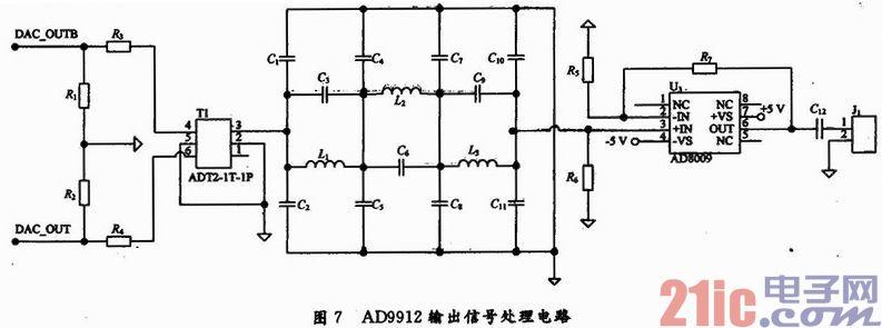
The output signal of AD9912 is differential signal, adopt the radio frequency transformer to change the differential signal into the single-end signal, and pass the low-pass filter circuit and power amplifier circuit to input to π network and compensate the network. AD9912 output signal processing circuit shown in Figure 7. Among them, DAC_OUT and DAC_OUTB are the differential signals that AD9912 outputs.
2.3 Signal Source Software Design The processor STM32F103 controls the output frequency signal of AD9912, mainly write the corresponding value into register of AD9912 through SPI.
Since a high-performance 25MHz constant-temperature quartz crystal is selected as the reference clock, the system clock PLL needs to be enabled. Bit 4 of register 0x0010 should be set to logic 0.
Registers 0x01A0~0x01AD are output signal control words, 0x01A0~0x01A5 are reserved registers, 0x01A6~0x01AB are frequency control words, and 0x01AC~0x01AD are phase control words.
The relationship between output signal frequency and frequency control word is:
fDDS=(FTW/248)fs(1)
Where: fDDS is the output signal frequency of the AD9912; FTW is the frequency control word; fs is the system clock frequency of the AD9912.
From equation (1):
FTW=round[248(fDDS/fs)](2)
For example, when fs=1 GHz, fDDS=19.44 MHz, FTW=5471873547255 (ie, 0x04FA05143BF7).
The relationship between the output signal phase and phase control word is:
△φ=2П(△phase/214)(3)
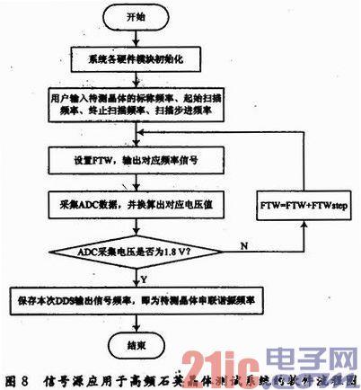
Where: △φ is the phase of the AD9912 output signal; △phase is the phase control word. Since the signal source needs to be applied to a high-frequency quartz crystal test system, it is not possible to output only a fixed-frequency signal, and a sweep signal must be output. Before the test, input the nominal frequency, initial scan frequency, end scan frequency, and scan step frequency of the crystal to be measured through the touch panel or touch screen. The processor calculates the scan step from the scan step frequency according to the equation (2). Control word (hereafter called FTWstep). Figure 8 shows the software flow chart for the signal source applied to the high frequency quartz crystal test system.
3. Experimental results The accuracy and stability of the signal source directly affect the accuracy and stability of the quartz crystal frequency measured by the test system. Therefore, the CNT-90 frequency meter is used to measure the signal frequency output from the signal source of this system. Experimental results show that the signal source output signal frequency accuracy is higher than ± 0.1ppm, the frequency stability is higher than ± 0.1ppm, the experimental data shown in Table 1.
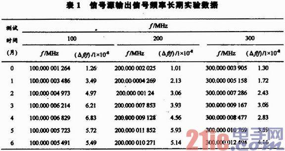
In the table, f is the set frequency value; f is the average frequency of the actual measurement; Δf/f is the relative deviation.
4. Conclusion This design successfully applied DDS technology to high-frequency quartz crystal test systems. A wideband signal source based on DDS technology is implemented. The signal source has the characteristics of wide output frequency range, high precision, high stability, high frequency resolution, and fast frequency switching, thus meeting the requirements of the high-frequency quartz crystal test system for signal sources.
Aluminium Die Casting for Communications Process flow chart
3D drawing analysis→material purchase→rough machine core &
cav→finish machine core & cav→machine electrodes→heat
treatment→linear cutting cavities→EDM cavities→machine mould
base→polish→assembly→mould test.
Aluminium Die Casting for Communications
1) Product Material: aluminum alloy, zinc alloy and aluminum profile
2) Surface Treatment: chrome plating, sandblasting, painting, anodizing, powder coating, electrophoresis.
3) Suitable for communications, auto parts, Lamp Part Series , water
pump part series, Power Tool Series, radiator part series, anti-static
flooring products and Other Series Products.
4) Whole process is done in house including: Tooling, Die casting, CNC
machining, CNC milling, Stamping, Plastic injection, Painting and
powder coating, Customized cub-assembly.
Our Advantages:
1) Experience in die casting for over 10 years and served customers all around the world.
2) More than 200 professional and hard working employees pursue a wonderful career.
3) International advanced-level equipment such as CNC, numerical
lathes, furnance, welding equipment, CMM and detect &testing
equipment we used to ensure our product`s(Aluminium die casting for
Communications) quality.
4) OEM service, you demand is our pursued.
5) ISO quality control
6) Standard: ASTM BS JIN DIN etc
7) Applied software for specification drawings: Pro/E, Auto CAD, Solid work, CAXA, UG. etc.
 |
 |
| One corner of CNC Workshop | One corner of Die Casting Workshop |
Based on high quality aluminium die casting for Communications, excellent service, reasonable price and timely delivery, we welcome customers, business associations and friends from all parts of the world to contact us and seek cooperation for mutual benefits.
Aluminium Die Casting for Communications
Aluminium Die Casting,Communication Boxes,Communication Accessories,Repeater Box Accessories
Ningbo Bowei Mould Metal Products Co., Ltd , http://en.bwmjyz.com