Photonics proposed three-dimensional micro-nano structure reconstruction method can be used for online detection

[China Instrument Network Instrument R&D] The rapid development of micro-nano devices in the fields of semiconductors, biological sciences and other fields has promoted continuous exploration and improvement of micro- and nano-structures. As an important measure of device performance, the measurement of three-dimensional topography of micro/nano structures has become increasingly important.


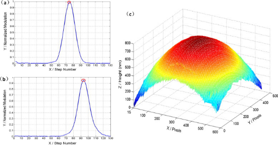
Time Domain Modulation Distribution Curves and 3D Topographic Reconstruction Results for a Single Pixel
Thanks to its tiny structure and sensitive quantum effects, micro-nano electronic devices have inherent advantages in information perception, material detection and so on. Compared with traditional devices, it has the advantages of high sensitivity, low energy consumption, small size and easy integration, and has a very broad market prospect.
Researchers at the Institute of Optoelectronics have proposed an algorithm based on white-light microscopic interferometry: a two-dimensional Fourier transform is used to acquire the frequency domain information of a single-frame interference image, extract the fundamental frequency spectrum for inverse Fourier transform, and finally obtain the time domain of the fringe. Modulation information. Through the high-precision scanning of piezoelectric ceramics, the modulation distribution of each pixel is obtained, and then the height information of a single pixel is obtained by using the extreme points, so as to realize the three-dimensional reconstruction of the micro-nano structure. The advantage of this method is that it can effectively eliminate the errors caused by the unfavorable factors such as unstable light intensity of the light source and external environmental interference, and improves the detection accuracy and system stability to a greater extent. It is expected to be applied to online detection in the future.
The project was supported by the Graduate Innovation Fund of the National Science Foundation for Nature and Optoelectronics.
(Original title: Optoelectronics has developed a three-dimensional reconstruction method for micro- and nano-structures based on white-light microscopic interferometry time-domain modulation)

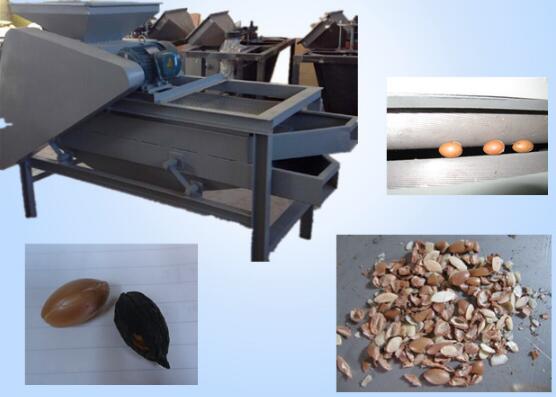
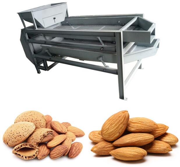
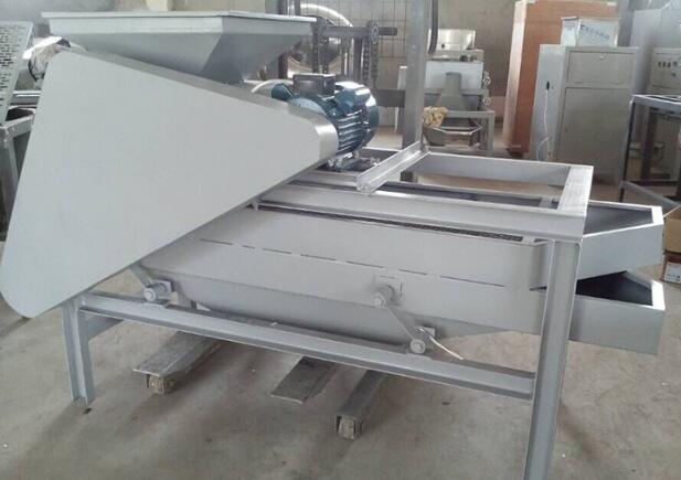
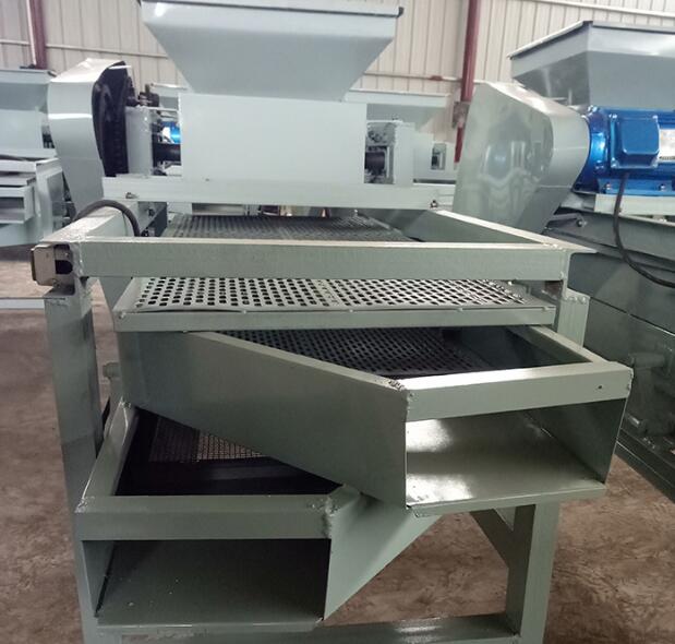
Grain Seed Palm Almond Walnut Apricot Sheller and Peller and Huller

A level of shelling, roller gap can be adjusted, apricot raw material size is not the same, take off the large adjustment gap and then take off as a cycle ..The roller gap should be 1-1.5mm smaller than the apricot kernel. (If apricot kernel size is mixed together, large apricot kernels have a 15 mm diameter in the flat, 12 mm in the flat, and a small 9 mm in the flat. Adjust according to the raw materials: 14 mm off the first roll gap. The large, large apricot nucleus is removed from the shell and the small apricot kernels are leaked at the same time. The apricot nucleus, which has been removed from the shell, is separated from the apricot kernel that has not been detached from the shell by a sizing screen under the shelling machine. Unopened apricot kernels, from the lower layer of the screen, the apricot kernel almond mixture after opening the shell, and then the second time to remove the roller gap 11mm off the third roll off the gap 8mm off Finished small, once finished. Reference, according to the physical material to adjust the gap to achieve no broken kernel as well,)


Technical Data:

Model

Productivity

(T/H)

Power

(kw)

Weight

(kg)

Dimension

(mm)

Sieve dimension Mark
HLD-300 3-5 2.5 260 1900X800X1250 / Environment friendly

Palm Sheller

Hazelnut Sheller

Nut Sheller

Apricot Sheller

Seed Sheller

Almond Sheller,Almond Huller,Corn Sheller Machine,Electric Corn Sheller

Hebei HELIDA Grain Selecting Machinery Technology Co., Ltd. , https://www.grainseedscleaner.com